Friday, October 25, 2013

Content Managment: Mercurial Tutorial

Mercurial on Windows Using Cygwin

1) Download and Install Cygwin

Download cygwin setup file setup-x86.exe (or setup-x86_64.exe) from http://cygwin.com/install.html and run it. You should see a windows similar to the one below


follow the guideline in installation wizard until you reach the package selection window as shown below


Select the following packages: 

a) openssh under Net (click on "Default" to change it to "Install") 
b) vim under Editors and 
c) mercurial under Devel.


Follow default options and finish install (this can take a while).

2) Create ssh folder and than create a separate folder to store class archive keys (useful when working with more then one repositories)

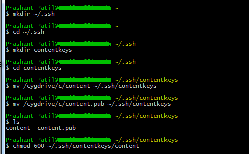
Open cygwin terminal (Programs - Cygwin - Cygwin Terminal) and type (refer figure below- key content with classes)

mkdir ~/.ssh

Command description:  mkdir is command to create new directory. "~/' is path for home directory and "." before folder name is used to create hidden directory (to windows explorer)

Navigate to this newly created folder by typing

cd ~/.ssh

Command description:  cd stands for "change drive" and used to navigate to a particular directory.

Create contentkeys folder inside newly created ssh folder

mkdir contentkeys

and navigate to this newly created folder by typing

cd contentkeys

Now, we need to copy the keys to this folder. First download the keys to C:\ and than execute the following command

mv /cygdrive/c/classes ~/.ssh/contentkeys
mv /cygdrive/c/classes.pub ~/.ssh/contentkeys

Command description: mv stands for "move" and used to move file from one location to other. Here we are moving the file from C:\classes (in cygwin windows c drive is accessed through /cygdrive/c/classes) to newly created classkeys folder.


You can check the content of this folder by typing command

ls

Command description:  ls stands for "list" and used to display the content of a directory
 
this will display the newly moved class and class.pub keys


Now, we will change the permission of the class key file by executing the command

chmod 600 ~/.ssh/contentkeys/content


Now we will create the directory were we want to save the mercurial repository. I am first creating directory "CBA" and then directory "content" inside it.

mkdir /cygdrive/c/Users/Prashant\ Patil/CBA
mkdir /cygdrive/c/Users/Prashant\ Patil/CBA/content


Now, we will clone the repository from the CBA servier to our local directory by executing the command

hg clone -e "ssh -i ~/.ssh/contentkeys/content"  ssh://hg@fab.cba.mit.edu:846/content /cygdrive/c/Users/Prashant\ Patil/CBA/content


Now, navigate to your arhive folder (in my case C/Users/Prashant\ Patil/CBA/content). You will find a .hg folder in it. Open hgrc file in notepad located inside .hg folder. Copy paste following (of-course edit it with your name and email). Don't remove which is already there in the file, just append this

[ui]
username = Prashant Patil
ssh = ssh -i ~/.ssh/contentkeys/content -C

[hooks]
changegroup = hg update >&2

Save the file and close it.

Now, in terminal cd to archive directory

hg pull

hg update

hg addremove

hg commit -m "message"

hg push

If branches have diverged, you need to merge them

pull

updage

merge

addremove

commit

push

If there are multiple heads then you need to merge them to a single head

hg heads 

hg merge headnumber

hg update -c

hg commit -m message
(repeat for every head you have created)

If two branches have incompatible changes and can not be merged then, save you updated file in location other then archive.

roll your archive back so that you can manually integrate your changes with those of whomever pushed their incompatible changes before you did!... 

hg commit --close-branch -m message 
hg update -c 
hg pull 
hg update 
hg merge 
hg add . 
hg commit -m message 
hg push 
(repeat for however many extra heads you've created) 


Mercurial in Windows using TortoiseHg

TortoiseHg is a version of the Mercurial application for Windows with GUI. 

Step - 1: Download executable from here and Install it.  
Step - 2: Create a folder where you want to keep all your files.
Step - 3: If you key is generated in openSSH then you need to first convert into putty (TortoiseHg) compatible key. For that you can use the software called Puttygen that can be downloaded from here
Step - 4: Now you  need to specify ssh keys. For that we are going to you a software called "Pageant". Navigate to C:\Program Files\TortoiseHg and double click on Pageant.exe . It will start running and you can find it in system tray in task bar.  Right click on system tray and click on "Add key" and add the converted ssh key.
Step - 5: Go to File -> Clone Repository. Enter Source "ssh://hg@fab.xxxx" and destination as one of the local directory in your computer.

 
Note - If you are asked for password then your ssh keys are not properly set. 

Step - 6: Edit configuration file - Go to file File -> Settings and select repository setting tab and click on "Edit File" and append following 

[ui]
username = Prashant Patil

[hooks]
changegroup = hg update >&2


Tuesday, October 22, 2013

Fablab Inventory Parts

1) Power Jack

Digikey Part#: CP1-023PJCT-ND


There are two stabs below the jack, remove it with wire cutter. The connection in board should be made one at the back(+) and one at the right end(-). both of these connection are not visible in above figure. 

2) Voltage Regulators

3) RGB LED 
Digikey Part#: CLV1A-FKB-CJ1M1FBB7R4S3CT
Datasheet here


4) Phototransistors NPN
a) Opaque -  OP520, digikey part# 365-1155-1-ND, datasheet 
Flat lense, opaque and spectrally matched to OP250, packaging - 1206
b) Clear - OP521 (clear)


c) OP522, datasheet.
Integrated narrow lens

The green mark indicate collector. The circuit is VCC-49K-Collector-Emitter-GND and voltage is sensed at collector pin.

5) PTC Resettable Fuses

PTC has conducting polymer consisting of carbon black particles. When the high current is allowed to pass, polymer expands increasing distance between carbon particles. This in turn results in increase in resistance.

Ihold (current usually drawn) - 500mA, Itrip (current at which it trips) - 1A

Digikey Part# F3733CT-ND  Datasheet.
Suitable for providing extra protection to USB port.

6) Buzzer
(ref)
a) Magnetic
- Narrow operating voltage (1V to 16V)
- High current consumption (30mA - 100mA)
- Low rated frequency, small footprint and low sound pressure level.
Magnetic inducers have inbuilt transistor to drive buzzer. Magnetic transducer doesn't have these transistor and hence external transistor is required.

Digikey Part# 668-1060-1-ND, datasheet


b) Piezo 
- Narrow operating voltage (3V to 250V)
- Low current consumption (less than ~30mA)
- High rated frequency, larger footprint and higher sound pressure level
Piezo transducer doesn't have electronic circuit and hence square wave is required. A piezo inducer has an in-built circuit and only DC voltage is required.


Monday, October 14, 2013

Eagle Tutorial

Setting-up Eagle for PCB Design

Step - 1: Download latest free version of Eagle from here and install it.

Step - 2: When you start Eagle, it opens a windows called "Control Panel" as shown below
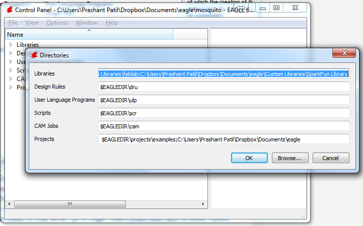
 Libraries are component library which you will use in project, Design rule is useful when you send board for manufacturing or mill and Projects is where you save all your projects.

Step - 3: Add frequently use libraries.
 Download some useful part library for eagle such as Sparkfun Eagle Library , fablab library and Adafruit library. As you will work along, you will make some modification to these libraries and you want to be able to access those library from any where. For this, I like to keep my library and Projects in my dropbox. Create a folder eag   le and a sub-folder "libraries". Copy the "Sparkfun" and "fablab" library folder in this folder. To add this folder to your library go to Eagle control panel then click on menu Option-Directories. In Directories windows, browse and select folder "Sparkfun", "fablab" and adafruit folders.  Do same for project directory.


Note - It is recommended to use mouse instead of laptop touch-pad.

Eagle Library Management


Important - In-order to use a library, right click the "SparkFun Library" folder and click "use all". You should see a "green bulb" in front of every library file indicating they are being used.
  1. Adding a Component to Library from other Library
    I prefer to keep my favorite components in one library so that they can be ready used. Usually, this involve copying a component from other library to your "favorite" library. To add component from one library to other. First open the library where you want to copy the component by double-clicking it. Then navigate to the "device" you want to add in library list, right click and click "Add to library". This will open the component in library editor. Here, you can edit the description and delete certain package associated with this device if you don't need them. To rename the component, in library editor go to Library--Rename and enter new name. Once you are done with edition click "save" in library editor to save component to new library. To change the symbol's prefix (e.g. IC1, IC2 for diodes or R1,R2 for resistors), click on Prefix and enter the desired prefix. To change pin names, you need to open symbol go to device -  symbol open it. Rename symbol, right click on any pin and rename it accordingly.
  1. Edition a Component in a Library
    First open the library by double clicking the name.lbr in control panel. Now in library editor go to Library-Devices select the device you want to edit and open it. The device will open in the library editor where you can edit it.
  2. Removing a Component from a Library
    Open the library in library editor by double-clikcing it. Then go to Library- Device/Package/Symbol (depending upon component) and open it. On the top of the library editor windows you will find the name of the file you just opened. Now go to Library-remove and type search filename and search than hit OK to remove. Click save icon in toolbar of eagle library editor. If you try using the remove option without opening a part from the library Eagle will throw you a “not found” error.

    In eagle library for every part you have, symbol+package+device file. Package is components footprint for PCBs. A device is for schematic and Package is for board. Device links the symbol and package and makes the whole part. To remove a component, you have to make sure you delete symbol and package and device associated with that component.
  3. Creating a part in library
    An eagle part consist of a symbol and corresponding package. The package is the footprint of the device in board. You make a "device" by linking a "symbol" and all its corresponding "packages". While making apart you can use preexisting packages such as SOIC8 etc. Information about the package can usually be find in the datasheet.


Schematic Design

Schematics should always be drawn on a grid of 0.1 inches (2.54 mm) since the libraries are defined this way. 

Rename part - Use name command click on the origin of the part and enter new name.

Change Value - To change value use value command click on the origin of the part and enter new value 

 To change the value and name of the component, first type "smash" then select a component. This will bring + near the corresponding name/value.  Use move command and click on + sign for moving name and components.


Board Design

To let eagle redraw the connection use "Ratsnest" tool from the toolbar on the left or "rats" command. For optimizing the PCB milling use the design rule Patil.dru which make sure the spacing between tracks and pads are 

Set the grid to 10mil while routing tracks. And visually make sure the distance between the tracks you draw is more than 1.5 grid size as that will be 15mil and the drill bit we will use is ~15.6mil. Offcouse check with "drc"using the Patil.dru to find any problems.

Resizing a rectangle - Type       "move" command and hold the "Ctrl" key while clicking on the box. This way you can re-size the rectangle. 

Once routing is done, optionally you can increase the width of track (~16mil) which are not tightly paced. Type change, select width and double click on the tracks for changing width. The track between the resistor can be changed to 16mil (check it)

when making the bottom box for final cutting of board, make sure that you keep atleast 20mil space otherwise fabmodules won't recognize it.

For boundary of the board, keep 40mil (not more) distance from the side tracks.


For exporting track, select top layer and export monochrome at 2000dpi


For exporting boundary, select bottom layer and Dimension layer. Make sure the blue box is inside the boundary and has 10mil boundary. 


Exporting Image for milling


Board Boundary - Select the layer - Top, Bottom and Dimension. Make sure that the rectangle in bottom layer at least have 40mil space from the tracks. Move the dimension rectangle such that the space between the bottom layer blue rectangle and dimension rectangle is 10mil (1box if grid is set to 10mil). 
Go to layer and select only bottom layer, Export monochrome at 2000dpi.


Layers in Board Layout Editor

1) Top - for tracks (red)
16) Bottom -
19) Unrouted track (yellow)
20) Dimensions - dimension of the board (white rectangular box)
21) tPlace -  which is used to draw lines that will be rendered as the silk screen on your PCBs (the printed text/lines/shapes we see)
23) tOrigins - origin of each component in top layer
25) tName - Name of each component (white) like R1 U$1 etc
27) tValue - Value of component in top layer (white) like 1K, 1uF etc (value set in schematic)
29) tStop - This layer is used for solder mask (hashed white boxes around pads)
51) tDoc - is used for documentation purposes, such as drawing the mechanical dimensions of your part. Normally this layer isn't printed on the PCBs, but it's very important for documentation and for PCB design.


Silk layer

Silk layer is useful while soldering the board. I prefer to keep only component value (as the unit already tells you the type of component) so disable the tName layer. Sometime value of two component overlap each other. To avoid overlap first click on smash button (or smash command), click on component when + sign appear click move and move the value to other location.


Library Editor


Editing footprint of a device

1) Double click on the library name in control panel to open it in library editor.
2) Go to Library - Device and open desired Device. In the left side of the window you will see various packages assosiated with this device. Right click the package you want to edit and click on "Edit Package"
3) To re-size pads, right click on pad,  go to property and enter new size.Once you've done that it will show up on all new boards and new placements
4) In order to update the board you've already started you need to select Library - Update all from the board window and all the footprints will be updated to the new one you've edited.

Creating a Part Libary

The part symbol should be made on 0.1inch grid because the schematic editor by default uses 0.1inch grid to place symbol in schematic.

File -  New - Library
save it as IC-icnumber-discription (just to that its easy to short later)
Symbol (for schematic), Package (footprint for board) and Device (co-relate symbol to package)
In library editor make sure grid is 0.1inch and visible.
2) Select "Wire" and make sure "symbol" layer is selected in the drop-down list. Make a rectangle with wire, 3) Put pin using Pin (select size to small in medium) and click both icon (for name and value). You can also select type of pin, by default its I/O pin.
4) Use Name command to assign meaningful name to each pin.
5) To assign name to newly created symbol click Text [T] icon, give it a generic name >Name so that eagle can automatically assign it a name. Make sure layer 95 Name is selected from drop-down list and put the text near the symbol.
6) For value to go Text, type value, select layer 96 Value and put it near the symbol >VALUE


PCB Milling Using Modella

Eagle Settings

Grid - 10mil 
Change the track width to 0.01inch (10mil) or 16mil. 10mil is ideal for small and dense board however, you might see some track coming out of board during debarring if board is large and not flat during milling. One good way is to first rout the board using 10mil and than change it to 16mil where space is available.

While routing make sure that you have at 1.5 to 2 box difference (16mil to 20mil space, drill bit for milling is 16mil)
In drc make sure that track width is set to 10mil and clearance between track is set to 16mil.
Type change in cmd and then select width
Export image in 2000dpi

Some important parts

FTDI header - M06SMD
01_Sparkfun -> M06 -> M06SMD


Modela

1/64inch = 15.6mil = 0.4mm

Schematic Design

Use "net" command to make electrical connection. Never use "wire" command.

Connecting pins of two IC by name - Some time in-order to have clean schematic and to avoid drawing many nets you may want to connect pins using name. To do this

1. Draw a very short net (using the net command) out from Pin 1 of IC1, double click at the end  to end net. Do the same for other pin also
2. Now select the NAME tool. Click on the little net you drew in step 1 and give it a name. Give the same name to other short net you draw on other pin. You will be asked if you wish to join the two nets together, say yes.
3. Select the LABEL tool. Click on each of the little nets and attach the labels.

Milling trouble shooting
1) Tracks thinner then expected?
Make sure you are exporting it at 2000dpi

2) Tracks are not smooth?
Make sure the modela plateform is tight and sturdy.

3) 


FAQ

1) Moving group - First type group cmd and use press and  drag method to group components , right click and select "move group"

2) Changing all track width. go to Edit-> channge a list will open at the bottom go to width and select desired width and than click the track who's width you want to change.

3) Alternate - altium

4)

" The same can be done for "User Language Programs" or, for example, for the "Projects"
branch. By the way: User Language Programs (ULPs) are more or less simple, C-like
programs that can be used for a variety of tasks. It is possible to export data from your
schematic or layout into any format. There is for example "dxf.ulp" which creates DXF
data or "bom.ulp" for creating a bill of materials"

"session"

Idea - circuit design - board design - fabricating board - testing - loopback or deploy

echo board, circuit diagram
 - microcontroller with reset circuit and crystal
- ISP connector
- FTDI serial connector

new project then new schematic - microcontroller power supply - rest circuit - crystal - programmer and ftdi connector.

Omax Abrasive Waterjet Cutting

 Introduction


Parts

  1. High Pressure Water Pump


    The pump screen is shown below


    Pressing the Up Arrow increases the pump’s RPM and water pressure. Down Arrow at any time decreases pump RPM and water pressure. Don’t touch these arrows under any circumstances.

DesignCAD Tutorial


1) Change the unit by clicking at the right/bottom of the screen and selecting "change units"
2)

1) Design using Inkscape, make sure to select inch as defalut unit so that its compatible with OMAX Layout editor.
2) Import


Note about designing in Inkscape

" While using saveas in inkscape, it assumes the dimentions are in mm. The import function in OMAX Layout assumes dimention in inches. So technically, 1mm in inkscape is equivalent to 1in in OMAX Layout edtior.

In Latest version of inkscape, while exporting use the base unit as the one you used in drawing, this will make sure that your part not get scaled in other when imported to other .dxf editors. To check import it to OMAX Layout and roughly check size. Each grid in OMAX Layout is 1".

For drawing "hollow circle" , select fill as none (bottom of the page) and stroke as black (for white background) and stroke thickness 0.001

Installing OMAX Software

Get .exe file from John D ( In my case I have V11 in my dropbox) and install it in your computer. This will install two programs 1) OMAX Layout which is used to .. and 2) OMAX Make

Creatig Toolpath


1) Import ".dxf" design file in OMAX Layout software. Roughly check if the dimension of your design is OK (one box corresponds to 1in). Press OK button

2) Assign Cutting Quality

Select quanlity of cut by clicl on "Quality" icon than select the desired quality number. Higher the number better it is. Usually, I use quality 3 as shown below


2) Right click on "Selecct" and than select All as shown below. Immidiately, all the curve in green will change to yellow indiating that they are selected for toolpath.


Operation

  1. Open the building’s inlet valve that provides water to the pump. (yellow valve image here)
  2. Turn the pump On/Off switch to the ON position (“I”).
  3. (confirm this step) Start the pump by pressing RUN button. Once the pump starts, verify that the red LED next to the Run button on the keypad is lit.
  4. When the pump stops, verify that the red LED next to the keypad’s Stop button is lit
  5. Turn the pump On/Off switch to its OFF position.
  6. Pushing the emergency stop switch in immediately shuts down the High-Speed Pump.

Don't forget to put abrasive material.
lower the spindle: Unlock from the center handle, lower using the upper rotating handle until itss free. Fromt the point it gets free, trace back to 180 degree.

Saturday, July 27, 2013

Serial Port Interface

Serial Port Programming Using Python in Windows


1 - Download and Install Python Installer from here. User the version according to your version of operating system.


2 - You can use python by running "Python (command line)" or "IDLE (Python GUI)" from All programs - Python.

2 - In order to invoke Python from the Command Prompt (cmd) you need to add ";C:\Python34" to the PATH environment variable.

To do this, 

Right click on "computer" , go properties select "advance system properties" than "Environmental Variables". In the "System variables" variable list,  select path from the list and add ";C:\Python34" 


 Now open command terminal and type python, you should see something like this


Now, come out of the python interpreter by typing the command 


exit()


3 - Download pySerial from https://pypi.python.org/pypi/pyserial . Unzip and copy pyserial-2.6 folder into C:\Python27 directory


4- Navigate to C:\python27\pyserial-2.6 using cd command

cd c:\python27\pyserial-2.6 

5 - To install pySerial, type the following command


python setup.py install


Now, to test the serial port interface with the micro-controller board, download term.py from the link "http://academy.cba.mit.edu/classes/embedded_programming/index.html". Navigate to the downloaded directory using the cd command. To run term.py type following command (replace COM10 by actual serial port number you find in device manager)

python term.py \\.\COM10 115200

You should get the following window and it should return what you have typed


/// Draft ///


 Reciever

Code in the micro-controller board continuously monitor the Tx pin of transmitter and waits for start bit (logic low). Once the start bit is observed it continuously samples 8 data bits. After transmitting 8 bits the transmitter sends one (or more) stop bits i.e. Tx pin is logic high. The receiver again waits for logic low (start bit) and the process is repeated for every character byte.

PC COM Port

PC's serial port uses RS232 standard for communication. For RS232 standard logic high is

 a signal voltage in the range of -3 V to -15 V (typically -12 V), and a logic low is between +3 V to +15 V (typically +12 V).  On the other hand for micro controller board logic high is 5V and logic low is 0V. For this reason an FTDI cable is used which convert RS232 high (-12V) into micro-controller logic high (5V).

synchronous (requires a synchronized clock between the transmitter and receiver) - See more at: http://embedded-lab.com/blog/?p=1296#sthash.VjIImNKO.dpuf
two modes of operation: synchronous (requires a synchronized clock between the transmitter and receiver) and asynchronous (no synchronization clock required). - See more at: http://embedded-lab.com/blog/?p=1296#sthash.VjIImNKO.dpuf

two modes of operation: synchronous (requires a synchronized clock between the transmitter and receiver) and asynchronous (no synchronization clock required). - See more at: http://embedded-lab.com/blog/?p=1296#sthash.VjIImNKO.dpufsdsdsd

Thursday, July 25, 2013

Servo Motor Controller

A servo motor has three wires, Black (GND), Red (VCC) and White (Control)

Black and Red wire is connected to ground and Vcc respectively and White wire is used to control the rotation of the servo motor.

Servos are controlled by sending them a pulse of variable width. The control wire is used to send this pulse. The servo expects to see a pulse every 20 ms. The parameters for this pulse are that it has a minimum pulse width (usually 0.5ms), a maximum pulse (usually 2ms), and a repetition rate (20ms). 

Given the rotation constraints of the servo, neutral is defined to be the position where the servo has exactly the same amount of potential rotation in the clockwise direction as it does in the counter clockwise direction.  The pulse width of neutral position is usually 1.5ms.

When these servos are commanded to move they will move to the position and hold that position. Servos will not hold their position forever though; the position pulse must be repeated (every 20ms) to instruct the servo to stay in position.

  When a pulse is sent to a servo that is less than 1.5 ms the servo rotates to a position and holds its output shaft some number of degrees counterclockwise from the neutral point. If a pulse larger than 1.5ms is sent, the servo will rotate clockwise to certain angle depeding upon the exact pulse width.

Figure below shows some sample pulse trains


Tuesday, May 21, 2013

E-beam Lithography Using NPGS System

Introduction  

The NPGS card connected at the back of the computer provides the voltage to X and Y scan coil of of the electron beam. It also provides TTL signal to the beam blanker. The beam blanker accepts 0V and 5V as trigger signal to blank the beam.

The NPGS software also communicate with XL30 ESEM software through serial port. The XL30 software accepts some command also known as "opcode" which can be used to remotely control the SEM microscope. The NPGS software can send command to XL30 software to read working distance (WD), move the stage, change magnification etc.  

Check List

1) Faraday Cup
2) Gold standard sample or 100nm colloidal gold nanoparticles (by from here . (Get 50nm colloidal gold nanoparticles as 100nm is too big). See SEM images at end

You can either use different stubs for Faraday cup, gold standard and your sample or buy e-beam lithography stub which as everything in one stub


You can buy this stub from here
 
2) 3% PMMA e-beam resist.
3) e-beam resist developer
4) Iso-propanol


1) Cleaning substrate 

1) Put Si substrate in spin coater vacuum chuck. Check if vacuum is holding substrate. Set the rpm at 500-600rpm, set timer to some large value say (10min) and start spin coater.

2) While sample is rotating, squirt acetone on substrate thoroughly from center to circumference. While continuing to squirt acetone, start also squirting IPA, this will make sure that you acetone doesn't dry before squirting IPA. Stop squirting acetone and continue to thoroughly was substrate with IPA. After that start squirting DI water and stop squirting IPA. After thoroughly washing with DI water, either increase the RPM to 4000 or use nitrogen gun to dry sample.

Step – 1: Sample Preparation

1) Spin coat 3% PMMA solution on silicon wafer at 4000rpm for 45sec. This will coat about ~300nm of PMMA on silicon substrate. It is necessary to have clean environment during spin coating otherwise one can observe strain due to dust particles on Si wafer. One can use disposable droppers to avoid dust particles during spin coating. Use the entire wafer as compare to small chips while spin coating. (Note that, PMMA coated wafers can be used for many months as long as kept in dark).
2) Bake the wafer on hotplate at 180C for 60s.
3) Scribe number 1, 2, 3 and 4 on the four corner of the sample just enough to only scratch the PMMA layer not the Si substrate itself. These scribes will be very useful later to focus the electron beam. You can also put 100-300nL of 50nm gold nano-particles at four corner, this will help you focus and condition electron beam.


Step - 2: Conditioning Electron Beam using Gold Standard

1) Change the setting of connector inside SEM so that beam current can be measured with external pico-ammeter. Since this disable automatic "sample touch alarm" be careful while moving samples.
2) Mount the sample on e-beam sample holder near the gold standard sample.  Put the sample inside the SEM chamber with working distance (WD) of ~5mm. WD determines largest patterning area. For small features use 30kv or more and spot size 1.
3)  To condition electron beam, navigate to gold standard sample and focus the beam. Adjust the astigmatism to get the best image at higher magnification (~1000,000x). With my system, the best image I was able to get is shown below


image here

Once the beam is conditioned, don’t change the focus setting from now onwards until patterning.


If you have an image of your sample holder then use it to navigate to Au standard sample. In my case Au sample is on the right side of the Faraday cup.

Step - 3:  Beam Current Measurement using Faraday Cup

1) Navigate to Faraday cup avoiding looking into the e-beam resist coated sample. 
2) To Focus on the Faraday cup don't use the normal control but change the z-height of the stage. 
3) Once the Faraday cup is in focus by changing sample stage height zoom into the black hole until the entire screen is black. Wait for 10 minutes to stabilize the beam in the Faraday cup and measure the current of ammeter.


Below is the Voltage/Spotsize and Current (as of 05/05/2014) for my XL30 system

kv  spotsize  current

10  
10  3 110.5pA


4) Enter this value into the NPGS software.

Step - 4: Writing Pattern

1) Navigate to one of the corner of the sample and focus by changing the z - value of the sample stage. Use the scribes you made on the surface of PMMA to focus.
2) In NPGS software go to Commands -> Direct Stage Control
The software will ask you to enter "rotation value". Hit Enter to skip that. The software will than ask you to focus on corner and hit Enter. This will collect the working distance. Repeat this step for all four corners. The software will that determine flatness of the sample surface. (you can skip this step if you don't have stage controller)
3) Turn on beam blanker and set the beam to "ON". 
4) Quickly navigate to the location you want to write and the set the beam in beam blanker to "EXT". This will give beam blanker control to NPGS software which by default blanks the beam. 
Note: Its good idea to set high contrast (~50) and low Brightness (~30) so that one can see the affect of e-beam exposure on PMMA during navigation.
5) Open the .rf6 file, enter the value of the beam current and select the desired magnification as indicated by maxmag or run file
6) In XL30 software, set Scan is as External XY.
7) Run the .rf6 file.The NPGS software will itself open the beam blanker and start writing pattern. This can be seen in ammeter as the current value increases from zero to finite value.


Step - 5: PMMA Development

1) Immerse sample in developer solution ( 3:1 IPA:MIBK) and put ultrasonic bath for 70 seconds.
2) Rinse sample with IPA and dry with nitrogen.
3) Post bake at 95 degree for 30 minutes in conventional oven.


Step - 6: SEM Imaging of Written Pattern 

1) Deposit 5nm of Au using Physical Vapor Deposition or Sputtering
2) For Imaging use 5kV and spot size - 3.
3) Ideally the detector should be TLD but I don't have that in my ESEM system.
Note - At higher magnification of about ~ 10,000 I could see the resist getting exposed and modified due to scanning (can be seen as a box in all the images below)


Recommendation to get fine Feature Size


- In general higher accelerating voltage will give least amount of back-scattering at the surface and consequently the smallest line-width


Advance Topics

Note – When writing the dual layer patter, the software communicate with XL30 software via serial port and changes the magnification by itself.


Appendix

1) SEM image of 100nm Au colloidal nanoparticles